PhotoMachining, Inc.
Contract Manufacturing
For our clients which have novel requirements that require proof of concept, we offer laser process development services on an hourly basis. We will work with you to determine an effective test plan based on our experience in a vast array of applications and unrivaled laser types at our disposal. All with a mind to reach your goals, whether reducing manufacturing costs, minimizing out of spec parts or environmentally friendly process. PhotoMachining will partner with you to determine a solution for your success.

Our experience in contract manufacturing and material processing covers several areas: Medical Device Manufacturing
Diabetes Test Strips Millions of test strips per day are manufactured with a large number of these using lasers to pattern an electrical circuit on gold coated polymer. Blood is drawn into the test strip where it reacts with enzymes and then electrochemical technology is used to produce a reading. This reading is correlated to a glucose value – the number seen on the reader display. The strip manufacturing process uses multiple layers of materials. While all of these different layers can be made using lasers, only the base material, made of a thin conductive coating on a rigid plastic, uses lasers in production because the other layers do not require the precision and can be stamped. UV lasers are used to etch electrodes into the conductor. Atomizers and Nebulizers Atomizers are used to break up a mist into its atomic components for analysis. Nebulizers are used to administer medication in the form of a mist into the lungs. Inhaled aerosol droplets can only penetrate into the narrow branches of the lower airways if they have a very small diameter – less than 5 microns. Otherwise, they do not travel far into the body and the effects are compromised. Nebulizers use liquid or powdered drugs which are loaded into the device upon usage. Screens with very small laser drilled holes then break up the liquid and mix it with air or oxygen to make the mist. There are usually a large number of these holes and the exact size depends on the drug being used and the symptoms being treated. Since they are disposable, the devices must be sold inexpensively. A typical device will have 500 to 1,000 holes less than 5 microns diameter (taper is actually helpful in this case), so fast beam steering is crucial. Microfluidics Microfluidics is a multi-disciplinary field encompassing physics, chemistry, engineering, flow dynamics and frequently biology. It deals with the manipulation and flow of gas and liquids in a miniature, typically sub-millimeter system. Although the flow properties are the same on both a macro and micro scale, factors such as surface tension, viscosity and even electrical charges become much more important on the micro scale because of the much larger surface to volume ratio. Even flow inertia is affected – inertia being much more important on the macro scale and having negligible effect on the micro scale. The channel diameter scale is in the range of 100’s of nanometers to a couple hundred microns. Because of this, larger designs cannot simply be scaled down, but instead new manufacturing techniques are called for in order to exploit the micro scale physical properties. Catheters and Drug Delivery A catheter is a flexible tube that is inserted into the body to allow for drainage, localized drug delivery or access by surgical instruments. Catheters are sometimes laser marked with graduations so the surgeon can determine precisely how far the insertion has progressed at any time. Drainage catheters do not require the small holes sizes and tight tolerances that drug delivery catheters require and the holes can usually be made by mechanical methods. Drug delivery catheters however require precise hole size and positioning so that the minimal amount of drug can be delivered locally without damage to the surrounding area. A range of polymers can be used as long as the material has biocompatibility, but the full device usually includes some molded plastic components and sometimes a guide wire or needle. Drug delivery catheters are generally meant to be used and then removed from the body. Holes can be placed longitudinally, spirally along the length or in a number of other different patterns and different diameter holes can be found on different potions of the device. Sometimes other areas of the catheter are also laser machined, for instance the tip. UV and/or short pulse lasers are used in this application. Microfilters The best example of a microfilter for medical applications is a blood filter. Silicone based filters are constructed by drilling a number of 3.5 micron diameter holes which selectively trap the white blood cells while allowing the red blood cells to pass freely. All of these microfilter applications have a few things in common. First, the size of the holes is in the range of a few microns to even sub-micron. Filters generally use through holes, but blind vias can also be drilled with sub-micron depth control and hole diameter repeatability. Aspect ratios of better than 10:1 can easily be achieved and the range of materials includes polymers, glass, ceramics and metals.
Fluid Metering Orifices A good example of a fluid metering device is a plastic injection molded part with a laser drilled hole for drug delivery. Injection molding is a rapid and relatively inexpensive way to make high volumes of disposable medical products, but the limitations on the molding process preclude molding holes small enough to serve as drug metering orifices – so lasers are used to drill these holes. First, the proper laser wavelength must be chosen so that a clean hole is drilled. Second, the required hole size must be achievable. UV lasers are the best candidates for most of these types of applications.
Marking Traceability is key in medical device manufacturing so marks (alpha-numerics, bar codes and 2D matrix codes) are used extensively just for identification purposes. The figure below shows two bar code marked products. The first is an identifier on a catheter. The second is an identifier on a polypropylene sperm storage vial – coding directly on the container can minimize the chance of mix up paperwork and surprising results! Marks can also be used as a part of the functioning product. For instance, it is possible to put graduations all the way around the circumference by spinning the part while the laser dwells for some time at each graduation location. Then, the part is stopped and alphanumerics are placed on one side to identify the graduation lines. In this case, the marks are part of the functionality of the device and not just an identifier.
Microelectronics and Semiconductors
Microvia Drilling PhotoMachining is the leader in supplying contract laser microvia drilling services and solder
The figure above shows some plated laser drilled microvias in FR4 (flame-resistant Class 4)material. This material is somewhat harder to work with than others in that it is inhomogeneous and the embedded fiber glass ablates at a much higher fluence than the epoxy matrix, but it is relatively inexpensive and is probably the most frequently used dielectric.
In the above figure, (a) shows 50, 75 and 100 micron diameter UV laser drilled vias in resin coated copper, while (b) is taken at an oblique angle. Homogeneous materials work much better for UV lasers than glass filled material since the glass is somewhat transparent at 355 nm. If done correctly, the UV light can clean the underlying copper such that no subsequent cleaning process is needed before plating, but in practice a cleaning step is usually performed. In fact, if short pulse UV light is used, 50 micron blind vias in circuit boards can be drilled at the rate of hundreds per second, with little or no heat affected zone and in any common circuit board material.
All of our lasers are networked to the Internet through our main server for easy file transfer. Please contact PhotoMachining Customer Service to get instructions on how to upload files to our system, via e-mail attachments or FTP. We will be happy to process your printed circuit boards as prototypes, small lots or on a recurring, high volume contract. Besides microvia drilling, we also do flexible circuit laser processing, dielectric material removal, photo resist removal and patterning, and a variety of other laser based processes. In addition, we can supply the following services:
Dielectric Removal from Conductive Surfaces Another active area is in removing dielectric materials from conductive surfaces. The fastest method of accomplishing this is to use a CO₂ laser which has the virtue of being almost completely reflective off of copper and therefore there is less chance to etch through underlying conductive layers. Because it is a thermal process, there is a HAZ around the edges and there may be debris that needs to be cleaned afterwards. More importantly, when the laser gets very close to the reflective copper surface, the long penetration of the 10 micron wavelength coupled with less than 100% absorption leave a thin residue on the surface that needs to be subsequently cleaned – however a cleaning process before plating is normal anyway. If a UV laser is used the copper surface is in principle clean enough for plating afterwards, but again a cleaning process is normal – especially if the subsequent plating does not take place immediately and oxidation occurs.
Solder Mask Removal Another opportunity exists in repairing engineering or manufacturing mistakes. For instance, solder mask is extremely hard to remove once it is applied – unless lasers are used, which makes the task pretty straightforward. Solder mask is put in the wrong places on a routine basis and there is cost associated with remanufacture – plus by the time the mistake is noticed, delivery may be impacted. Therefore, lasers can be used to both minimize rework costs and to achieve on time delivery.
ITO and Conductive Metal Structuring Lasers work extremely well in the patterning of ITO films and such devices are used in flat panel displays, touch screens, instrument displays and some medical devices. Lasers are used to isolate certain portions resulting in an electrical circuit. Green (532 nm) lasers are very interesting especially for use on displays as the substrate is usually transparent in the visible portion of the spectrum. Therefore, no damage is done to the underlying substrate. If a large amount of material is to be removed on for instance a glass panel, it can be done by lasering through the glass with the ITO face down, resulting in no generated debris being deposited on the surface of the part. For smaller spot sizes on target, 355 nm also works well.
Wire Stripping
Defense / Aerospace There are a host of applications using lasers in the defense and aerospace fields that cannot even be discussed because of their proprietary or sensitive nature. Lasers are nevertheless used for welding, drilling and cutting thick metals and composites, marking and repair. The big application is in the manufacture of jet aircraft engine parts, but other hot topics include sensors, RFID identifiers, range finding, missile guidance and defensive lasers. Services applying to defense and aerospace include:
Renewable Energy In the renewable energy (or even energy conservation) areas, lasers are used from the far IR to the UV in many different aspects of manufacturing. In the case of energy production, lasers are used to manufacture the devices which provide the power (for instance solar panels) and that store the power (batteries).
Other Applications
|
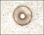
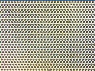 An array of small holes (10 micron) drilled using an excimer laser and multiple hole imaging mask. By stepping and repeating, this procedure can produce very large filters, on the order of 300 mm across.
 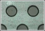 Fragment of an array of 100 vias 75 microns in diameter in 15 microns thick plastic wall.
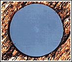
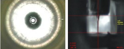 Orifice in a plastic part 550 microns thick, 25 microns in diameter: (left) top view; (right) side view.
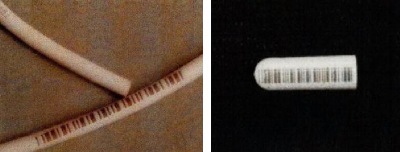 (Left) Bar code on catheter; (Right) bar code on polypropylene vial.
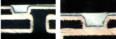 Plated laser-drilled microvias in FR4.
 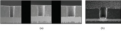 Photos courtesy of Hitachi
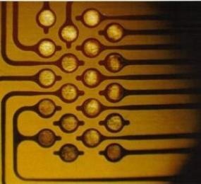 Flexible circuits are the most common products that have laser ablated conductive pads. The figure to the left shows excimer laser removal of polyimide coated copper using mask imaging to expose all the conductors simultaneously. This product was done on a roll-to-roll machine.
 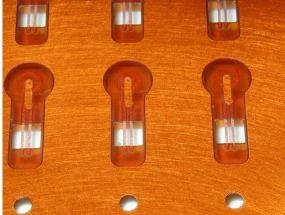 This figure shows conductors exposed using a CO₂-TEA laser.
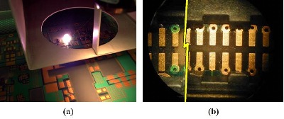 Here (a) shows a CO₂-TEA laser removing solder mask from a printed circuit board while (b) shows the end result with the untouched section on the left and the laser processed section on the right.
 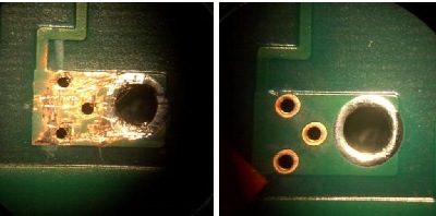 This figure shows the result when one tries to mechanically remove solder mask (left) and the same mask removed by a laser (right).
 This photograph shows ITO removal from glass. The line width is about 25 µm; the patterning is invisible to the naked eye.
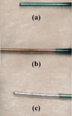 The figure to the left shows an unprocessed (a), laser stripped (b) and tinned (c) wire.
 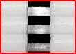 Larger diameter wires can be ‘stripped’ with a CO₂ laser in a two step process. This figure shows a set of conductors exposed on both sides using a 20 W CO₂ laser. First, the insulation is removed on one side, then it is turned over and the process is repeated. Round wires can be cut around the circumference and then the insulator is manually removed. If a stripped section is in the middle of the wire rather than on the end, a longitudinal cut is made so the insulation can be removed. If the wire and insulator are thin enough, lasers can be used to completely remove all the material without a secondary manual step. This is done using either a CO₂-TEA laser or an excimer laser.
 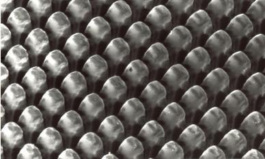 Three-dimensional structure in polyimide.